Archives for posts with tag: Renewables

The IEEE Photovoltaic Specialist Conference (PVSC) is renowned as one of the world’s largest photovoltaics (PV) conferences. It is also probably the oldest conference that is still been held annually. I was fortunate enough to have the opportunity to attend the conference this year, for the second time.

As the PV energy market is evolving from niche to mainstream, I’ve noticed some shift of focus in the topics of this year’s conference. The most noticeable would be the emphasis on the long-term reliability of PV systems. The very first plenary session on Monday morning was dedicated to PV reliability issues, with two talks covering both modeling and analysis of data collected from real field operations.

While crystalline silicon is still the dominant technology, exploration into new materials and concepts has never been slowed down. It is the same with this year’s conference. It is my area of interest to discover potential new technologies that can bring fundamental improvement to the conversion efficiency of the solar cells, or dramatically reduce the cost per watt. I’ve noticed that there was a session dedicated to III-V on silicon solar cells. This is very exciting since I’ve been working in the same area for nearly my entire postdoc period. Previously there has never been a separate session for this topic. Although still nothing revolutionary was reported even with a dedicated III-V on Si session, at least it shows that people are realizing the great potential of substituting expensive III-V or Ge substrates in a traditional multi-junction solar cell with a much cheaper Si substrate.

To give more insights on the latest development in this area, I have summarized some of the highlights from the III-V on Si sessions. The most noticeable one would be the big picture outlined by Alexander Haas et al. from Emcore and Ohio State University. They predicted 39% efficiency in the near-term for III-V on Si 3J solar cells with active Si bottom cells, and GaAsP and GaInP top cells, grown by monolithic approach, with GaP and GaAsP graded buffers between the GaAsP and Si sub-cells. In my opinion, this efficiency is shockingly high considering that the most successful monolithic multi-junction solar cells involving Si as the active cell reported so far are only 21% in efficient [1]. If it is true that 39% can be achieved in the near term, this may be one of the most exciting breakthroughs in multi-junction solar cell development in nearly two decades!

On the more practical experimental front, Andreas W.  Bett’s group from Fraunhofer reported that direct epitaxial growth of a GaInP/GaAs dual-junction solar cell on a GaAsxP1-x buffer on silicon yielded a 1 sun efficiency of 16.4% (AM1.5g), and a similar device fabricated by semiconductor wafer bonding on n-type inactive Si reached already efficiencies of 26.0 % (AM1.5g). S. A. Ringer et al. from Ohio State University and University of New South Wales are tapping into the field of transitioning the buffered growth technique of GaInP/GaAsP on Si from MBE to MOCVD for potential high volume production capacity. More details on this topic can be found in references [2-4].

Among some other sessions that captured my attention, one would be the Fundamental and New Concepts session on Tuesday afternoon. Dr. Alex Zunger from University of Colorado presented a systematic approach to identify new PV materials with suitable properties. He proposed to filter candidate materials from tens of thousands of possible materials combinations from the periodic table with a first principle approach and then try to experimentally synthesize these candidate materials. As a promising example, he and his collaborators have succeeded in discovering a new transparent conductive oxide (TCO) material with this approach. See reference [5] for more details.

Also, as one of the best student presentation award finalist, Aaron Martinez from Colorado School of Mines presented his results on the synthesis of silicon clathrates. This material is essentially Si, but with a very special crystal structure, neither diamond structure nor amorphous structure as is typical. The most attractive feature of the silicon clathrates is that it can be tuned into a direct bandgap material, which means dramatically improvement in the efficiency if the material can be made into a perfect shape. Interested readers can find more details in reference [6].

There were a lot of takeaways from this conference. Tampa is a beautiful city with nice communities and beaches. This was an unforgettable experience.

Jingfeng's picture

-Jingfeng Yang

Research Associate

Department of Engineering Physics

McMaster University

References

[1] M. Umeno et al., Solar Energy Materials and Solar Cells, vol. 50, pp. 203–212, Jan. 1998.

[2] A. Haas et al., PVSC 39, Area 3-246, June 18, 2013

[3] F. Dimroth et al., PVSC 39, Area 3-245, June 18, 2013

[4] S. Ringel et al., PVSC 39, Area 1-942, June 21, 2013

[5] A. Zunger, PVSC 39, Area 1-235, June 18, 2013

[6] A. Martinez et al., PVSC 39, Area 1-236, June 18, 2013

The 39th IEEE photovoltaic specialist conference was held between June 16th and 21st at the Tampa bay convention center in Tampa, Florida. It was a congregation of industry experts, and research giants. Researchers from NREL, Sandia National Laboratories and Universities across the globe graced the occasion to present their latest studies on photovoltaic system design, implementation and reliability of on-sun PV modules.. The program was significantly all encompassing. Besides the presentations, social activities and mixer programs were held to allow attendees to interact, network and share knowledge. Of notable interest was the presentation of the cherry award to Keith Emery. Previously unknown to me, I found that he is renowned for his contribution to photovoltaic research for his design, development and implementation of IV characterization methods. He pioneered the first generation of hardware, software and procedures to measure current-vs.-voltage characteristics as a function of temperature, spectrum and intensity for single and multi-junction cells and modules.

Oral and poster presentations at the conference were grouped into eleven categories which ran in parallel beside keynote or plenary sessions. Personally, I attended sessions in the categories of advanced PV module concepts and designs and PV modules and terrestrial systems. From the presentations, I deduced that there is a significant amount of attention being given to system performance evaluation and energy yield assessments of photovoltaic systems. As such, there is a growing interest in research on concepts for data collection which is a necessary input for energy assessments. There were also presentations on the design of experiments for photovoltaic system assessments. Particularly, I found some modeling techniques used to evaluate PV system performance to be of interest. A few of them include:

Validation of the PVLife Model Using 3 Million Module-Years of Live Site Data [1]

In this article, SunPower corporation (the manufacturers of SunPower PV modules) presented their experiments and results on long term system degradation analysis. An interesting fact is that they performed their analysis using a relatively new approach. Rather than using high fidelity diagnosis methods, they settled for noisy large statistical samples that represent records from a large number of installed systems to estimate the median system degradation rate of PV modules. As a key player in the PV module industry, the company aimed to consolidate their understanding and confidence in system degradation trends and hence they’ve developed a model called the “PVLife model” which is used to simulate module degradation characteristics. Their PVLife model operates with inputs of weather data and cell characteristics to determine degradation factors such as UV induced cell degradation, encapsulant browning, bypass diode and solder joint failures.

For comparison, degradation analysis was carried out on a total of 445 systems.  226 systems were comprised of SunPower modules which had an installed capacity of 86MW. These systems had been operating for up to 5.5 years.  There were also included 149 systems of non SunPower modules which were as old as 11.5 years with an installed capacity of 42MW. Altogether, the total fleet-wide modules representing 3.2 million module-years of monitored data were used to determine degradation rates. Following a plethora of statistical analytics, they found the PVLife model to be in very good agreement with the compared module degradation rates. It was further claimed that the model results were used to develop better modules with lower degradation rates. Attention was focused on the relationship between degradation rates and the placement of the module contacts. According to their studies, it was found that front contact modules for a variety of reasons had a higher degradation rate when compared to back contact modules.

Overall, the work by SunPower suggests that they have successfully developed a working system to model the degradation mechanisms due to several factors in PV system operation. Validation of its results against a large dataset of on-sun measurements was shown to be in very good agreement

Simulations of Energy Yield Improvement in Utility-Scale PV Plants Using Distributed Power Point Trackers [2]

Researchers from First Solar Inc. presented their research on the use of distributed maximum power point trackers (MPPT). It was identified that any energy losses in utility scale PV installations decrease the financial value of the system. They aimed to analyze methods that might reduce the losses in utility scale PV installation such as partial cloud cover induced mismatch loss in the system. Since similar loss mechanisms due to building shading has been analyzed in detail, their focus was directed at non-uniform irradiance patterns created by cloud edges on utility-scale PV installations.  A model was developed to simulate the mismatch loss. The model simulates a PV array with a variable number of strings on a mounting structure. It simulates the movement of a cloud edge over the PV array whilst outputting the array IV characteristics based on voltage and current relationships. A study was then conducted on varying string lengths in the arrays for 10 and 15 modules in a string. Results from the analysis using their model showed a decrease in net energy loss when multiple maximum power point trackers were used. The key energy losses were found to be dependent on the length of the cloud edge. Measurement of the cloud edge in correlation the utility –scale system performance was prescribed to be conducted to further assess the impact of distributed MPPT in decreasing net energy losses.

Overall, the conference was a great learning experience. Its success encourages me to look forward to the next annual conference, which is scheduled to be held in Denver, Colorado

Jafaru Mohammed's picture.

-Jafaru Mohammed

M.A.Sc Electrical and Computer Engineering

Department of Electrical Engineering and Computer Science

SUNLAB Research Group

University of Ottawa, Canada.

References

[1]         E. Hasselbrink, M. Anderson, Z. Defreitas, M. Mikofski, Y. Shen, S. Caldwell, D. Kavulak, Z. Campeau, D. Degraaff, S. Corporation, R. Robles, and S. Jose, “Validation of the PVLife Model Using 3 Million Module-Years of Live Site Data,” in Photovoltaic Specialists Conference, 2013. PVSC’13. 39th IEEE, 2013.

[2]         A. Pope, J. E. Schaar, M. Schenck, F. Solar, and S. Francisco, “Simulations of Energy Yield Improvement in Utility – Scale PV Plants Using Distributed Maximum Power Point Trackers,” in Photovoltaic Specialists Conference, 2013. PVSC’13. 39th IEEE, 2013.

I had the opportunity to go to PVSC 39 in Tampa, Florida with fellow Highly Qualified Personnel (HQP). There were a lot of interesting speeches but I will only focus on a couple of them here – particularly those focusing on CdTe thin films progress. CdTe is one of the most attractive materials for production of low cost thin film solar modules [1]. The record efficiency for CdTe solar cells has been established to be 16.7% for 10 years. In the past 2 years, the CdTe record was broken several times and increased from 16.7% to 18.7%. However, there has been no significant change in the open-circuit voltage which was in the range of 840-860 mV for over 20 years. Many arguments have been made to justify the apparent Voc limitation, most frequently: poor hetero-interface with CdS, the difficulty in doping polycrystalline CdTe, midgap defect levels, or non-uniformities at the nano- or micro-scale. Paths for open-circuit voltage above 900 mV are:

  • Doping: Increasing doping level of CdTe is believed to increase the built-in potential and reduce recombination at the back-surface. Present doping levels are of the order 1014 /cm3 and different ways are proposed to increase them.
  • Lifetime: Higher lifetime(s) are expected to be a sign of less recombination in the junction and quasi-neutral region, and, hence, improved Voc and carrier collection. With higher lifetime, it is expected that a greater fraction of the recombination may occur at the back-contact due to increased electron diffusion through the absorber.

Gloeckler from First Solar announced a new record efficiency of 19.1% for CdTe, although not yet certified by NREL.

Despite these promising results, the gap between solar cell and module efficiencies is still wide (3-5%) [2]. This so-called “solar gap” constitutes a major challenge for commercial viability of photovoltaics. One explanation, proposed by M. Alam and his group at the University of Purdue, says that the “solar gap” is due to the monolithic series connection of thin films that causes shunt leakage current. Analysis of the shunt leakage current show that an I-V curve can be modeled by the diode equation and the shunt current, which has a non-linear relation with the voltage, as shown in Fig. 1. It was shown by Alam et al, that as a consequence of the series connection of cells, large shunts have a twofold impact on module performance. First, they modify the operating point of their neighboring good sub-cells, thereby lowering their output power. Second, a large fraction of this (already reduced) power, generated by the neighbours, is consumed by the shunted sub-cell. Interestingly this phenomenon is not unique to CdTe photovoltaics but more of a universal phenomenon and studies on CdTe, CIGS, OPV and amorphous silicon thin films show the same behaviour. At PVSC they have described a post-deposition scribing technique for electrically isolating these distributed shunts in monolithic thin film PV modules. The localized scribes minimize the losses due to defective shunts by restricting lateral current drain from its (otherwise defect-free) neighbors.

Figure 1 of Ahmed's blog

Fig. 1 Measured IDark (squares) can be represented by a parallel combination of diode with series resistance I (green), and a parasitic shunt component (red), with a symmetric (around V = 0) non-Ohmic voltage dependence. Reproduced from [3] with permission of The Royal Society of Chemistry.

References:

[1] W. N. Shafarman, “What’s next for Cu(InGa)Se2 Thin Film PV: Opportunities and Challenges”, 39th IEEE Photovoltaic Specialists Conference, 2013

[2] S. Dongaonkar, M. A. Alam, “Reducing the Cell to Module Efficiency Gap in Thin Film PV using In-line Post-Process Scribing Isolation”, 39th IEEE Photovoltaic Specialists Conference, 2013

[3] S. Dongaonkar, S. Loser, E. J. Sheets, K. Zaunbrecher, R. Agrawal, T. J. Marks, and M. A. Alam, “Universal statistics of parasitic shunt formation in solar cells, and its implications for cell to module efficiency gap,” Energy & Environmental Science, vol. 6, pp. 782–787, 2013

Ahmed Gabr's picture

-Ahmed Gabr

Ph.D Candidate, Year 3

SUNLAB, University of Ottawa

I recently had an opportunity to attend the 39th IEEE Photovoltaics Specialists Conference in Tampa, Florida (http://www.ieee-pvsc.org/PVSC39/). Since I am just starting to work in Photovoltaics, it was a great opportunity for me to get immersed in this very quickly developing field by listening to high quality presentations given by the leaders of the field. The presentations were divided into 11 topic areas, with a few sessions taking place at the same time. I really wanted to be in a few rooms simultaneously, but with my background in quantum theory I decided to focus mostly on attending sessions from research Area 1: Fundamentals and New Concepts of Future Technologies.

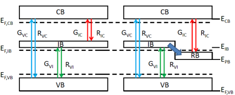
I found a talk by Megumi Yoshida from Imperial College London :“Progress towards Realizing Intermediate Band Solar Cell – Sequential Absorption of Photons in a Quantum Well Intermediate Band Solar Cell” particularly interesting. I was familiar with the concept of introducing the intermediate band (IB) into the solar cell to improve the absorption of photons with energy lower than the band gap energy (see Fig 1 (a)), however this talk took this concept one step further. The intermediate band solar cell (IBSC) can be created introducing quantum mechanically confined structures such as quantum wells and quantum dots [1] into the solar cell. In such cases, the IB arises from the confined states of the electrons in the conduction band (CB) potential.  In theory, by introducing the IB the current can be enhanced by two step absorption of long wavelength photons without reducing the voltage, hence leading to higher conversion efficiency (thermodynamical limit of 46.8% at 1 sun [2]), than a single bandgap solar cell (31.0% at 1 sun).

Figure 1 of Anna's blog

Fig. 1. Energy diagram of an (a) IBSC and (b) IBSC with photon rachet band (RB), in which extra photocurrent is produced due to sequential absorption of sub-bandgap photons increasing theoretical limit in the conversion efficiency. Reprinted with permission from [3]. Copyright 2012 AIP Publishing LLC.


However, experimentally obtained IBSCs suffer from a significant voltage loss resulting in lower than predicted theoretical conversion efficiency due to the short lifetime of electrons in the intermediate states. The short lifetime is caused by fast radiative and non-radiative recombination of carriers that occurs before the second photon can be absorbed. To achieve a long carrier lifetime of electrons in the IB, the authors suggest the introduction of a non-emissive (optically decoupled from the valance band (VB) [3]) “ratchet band (RB)” at an energy interval ΔE below the IB (shown in Fig. 1(b)). If there is fast thermal transition between the IB and the ratchet band, the photo-excited electrons in the IB rapidly relax into the RB where the lifetime of the carriers can be very long given that the RB is optically isolated from the VB. The increase in lifetime of the electrons enhances the probability of the second optical excitation process from the RB to the CB and increases the IB-CB generation rate. At the same time, the recombination rate of the electrons from the IB to the VB depends on the population in the IB. The presence of the RB reduces the population of carriers in the IB and the same the recombination rate leading to the increase of the photocurrent of the solar cell and its higher efficiency.

Figure 2 of Anna's blog

Fig. 2. Efficiency limit of photon ratchet IBSC of various concentrations as a function of ΔE. Efficiency at ΔE=0 corresponds to conventional IBSCs. Reprinted with permission from [3]. Copyright 2012 AIP Publishing LLC.

Authors calculate the globally optimised limiting efficiency of the photon ratchet IBSC as a function of the energy difference ΔE between the IB and RB. These dependencies are plotted for three solar concentrations in Fig. 2. Even though electrons lose the energy ΔE by transitioning from the IB to the RB, an increase in efficiency is visible as ΔE is increased. At the same time, the presence of the ratchet increases the below-bandgap and thermalization losses, but the associated efficiency gain through reduction in recombination is even larger. At 1 sun illumination, the efficiency of the IBSC is increased from 46.8% (ΔE = 0, conventional IBSC) to 48.5% with a photon ratchet at ΔE = 270 meV. At full concentration however, the introduction of the loss due to the presence of the ratchet band is not compensated by any other mechanism, leading to a decreased efficiency of the IBSC with the RB as compared to the standard IB cell (ΔE = 0).

Although it seems that the implementation of the photon ratchet IBSC is going to be challenging, I think that this concept is very interesting. Authors suggest that the RB can be built out states of indirect bandgap semiconductor separated in momentum space from the IB. Electrons would be first excited into a direct IB state, followed by a relaxation down through phonon emission to an indirect photon ratchet state, which is at a lower energy and separated by momentum k from the IB state, as well as the top of the VB.

Anna Trojnar's picture


-Anna Trojnar, Ph.D

Postdoctoral Fellow

Sunlab, University of Ottawa


[1] A. Marti, L. Cuadra, A. Luque, “Quantum dot intermediate band solar cell” Conference Record of the Twenty-Eighth IEEE Photovoltaic Specialists Conference, p940 (2000).

[2] A. Luque and A. Martí, “Increasing the efficiency of ideal solar cells by photon induced transitions at intermediate levels”, Phys. Rev. Lett. vol. 78, p5014 (1997).

[3] M. Yoshida, N. J. Ekins-Daukes, D. J. Farrell, C. C. Phillips, “Photon ratchet intermediate band solar cells,” Appl. Phys. Lett. vol. 100, p263902 (2012)

The 39th Photovoltaic Specialists Conference in Tampa, Florida was a great conference. Photovoltaic specialists from all over the world gathered at the paradise of recreation, learning the most recent developments in this field delivered by hundreds of high quality presentations and posters. The topics span across eleven general areas from fundamental and new concepts of PV to the supporting of PV innovation with little to none overlap between each area. For me, an organic chemist focusing on developing new polymers to improve the stability of organic photovoltaics (OPV), the area that mostly interested me was, without a doubt, OPV.

Thursday of last week was the day for OPVs. In the morning, Professor Christian Körner from Heliatek GmbH gave a talk on the recent progress of organic solar cells [1].  Like a typical general review of this field, the talk started with some fundamental concepts and theories of organic semiconductors, then moved to some developments that aimed at solving the issues commonly encountered when applying organic materials to photovoltaic devices. He also covered recent improvements on the lifetime and module efficiencies of OPVs, which are not as much discussed as the efficiencies of lab scale devices. Not surprisingly, the materials presented in this talk are highly related to those being developed at Heliatek. With active materials based on small molecules and p-i-n structured devices, they could achieve 12% of photo conversion efficiency on lab scale devices and 9% on 100 cm2 scale modules that last as long as several thousand hours under intensified illumination. However, from an academic point of view, these technologies and accomplishment do not necessarily reflect the general recent progress of OPV in academia, where polymers and bulk heterojunctions are the dominant materials and device structure, respectively. Regarding the progress of OPV using conventional structures and material, there was an interesting presentation in the afternoon session given by an award winning Ph.D. candidate Biswajit Ray from Purdue University [2]. In his research work, he showed that the limiting factor of the charge transportation process are recombinations happening at the neutral, flat region of the band diagram. Conventionally, many people think the limiting factor is charge mobility. Although his evidence is not sufficient enough, it is helpful to look at a problem from a view that opposes the convention.

Apart from the presentation content, a new presentation technique was unveiled at one of the plenary talks. In it, the presenter used a facebook homepage to deliver his talk with the aid of the timeline function. At the end, an internet address that directs to that facebook page made all the slides publically accessible. It is notable that people’s attention was drawn to this presentation even though some of them were not familiar with the field.

It was a wise idea that the conference committee chose to hold it in Tampa Bay. It was the best time of the year to go there and to the beach where the water was warm and the sand was fine and soft like snow. Everyone from the network that went to the beach had a wonderful time there. Also, the Salvador Dalí Museum is definitely worth seeing, since it holds the largest number of Dalí’s masterpieces which will truly stun you.

[1] C. Körner, M. Hermenau, C. Elschner, C. Schunemann, S. Mogck, M. Riede, K. Leo, “Recent progress in organic solar cells: From a lab curiosity to a serious photovoltaic technology” in 2013 39th IEEE Photovoltaic Specialists Conference (PVSC), 2013.

[2] B. Ray and M. Alam “Role of charged defects on organic solar cell performance: Prospect of Heterojunction-free device design” in 2013 39th IEEE Photovoltaic Specialists Conference (PVSC), 2013.

Ben Zhang's picture

Chi Zhang (Ben)

Ph.D. Candidate, Year 3

Simon Fraser University, Burnaby, British Columbia

As Ontario’s flagship renewable energy (RE) incentive program, referred to as the Feed-in Tariff (FIT), enters its third review, it is an appropriate point to assess several recent political and policy changes which have implications for the next iteration of RE incentives. In my previous blog, I wrote about the challenges facing Photovoltaics (PV) with respect to the World Trade Organization’s (WTO) initial ruling against Ontario’s domestic content requirements, growing economic turbulence in the RE sector, political adjustments within the provincial Liberal party  as well as other industrial and policy factors that have created uncertainty surrounding the future deployment and development of PV in Ontario. These events have had lasting impacts on the prospects of PV and continue to influence future policy engagement. In conjunction with prior developments, there are new pressures and policy changes which will have serious implications for PV. Do these changes point to positive change for the future of PV?

Foremost among these pressures is the fallout around the WTO decision. In May 2013, the final ruling by the WTO stated that Ontario’s RE policy framework was in violation of international trade law[i]. The decision established that the domestic content requirement, which requires that developers source a certain percentage of RE system components from Ontario companies in order to be eligible for FIT incentives, contravenes international trade agreements. Without protection from international competition, PV companies who have invested in Ontario face an uncertain future. Will PV panel manufacturers be able to compete with Asian firms? Which parts of the PV value chain will Ontario firms occupy? Will we purchase technology from overseas and focus primarily on project installation? These are just some of the questions left unanswered as the government begins to reinvent the FIT.

The provincial government has already communicated significant changes to the FIT, which may portent further revisions presently being contemplated. In June 2013, the government announced that large RE projects (>500 kW) would no longer fall under the FIT mechanism[ii]. Instead, these projects would be contracted using a competitive procurement process. The details of this process have yet to be articulated. Moreover, the annual cap for FIT contracts has been reduced from 250 MW to 200 MW[iii]. Aside from the FIT, the political administration has also renegotiated its deal to procure a significant quantity of RE from Samsung, cutting the contract from 2,500 MW down to 1,369 MW[iv]. From this, it would appear that a deliberate effort is being made to slow further RE procurement and deployment in the province.

Political pressures are also quite notable. First there is the continued uncertainty arising from a minority government situation, where opposing parties have stated they would either abandon[v] or seriously redesign[vi] RE policies. Second, controversial gas plant cancellations continue to plague the governing party, casting shadows over the energy file and the commitment to RE deployment[vii]. Lastly, and perhaps most importantly, there are still many unanswered questions regarding the future of nuclear energy in the province[viii]. If Ontario commits to build new nuclear reactors, there is little impetus to invest in RE and efficiency.

Together, the above factors indicate that there is increasing uncertainty surrounding the RE sector in the province. Recent developments suggest that Ontario is veering away from its commitment to an economy and energy system based on RE. So, the worst may have yet to come for PV in Ontario.

Danny Rosenbloom

Daniel Rosenbloom
Ph.D Candidate

Carleton University


The Photovoltaic Specialist Conference (PVSC) offers a tremendous opportunity to any photovoltaic (PV) oriented researcher both young and old to convene at a single location and share their latest research results, meet new researchers and potentially new collaborators, catch-up with old colleagues or previous acquaintances in the field, and finally, keep up to date on the recent progress in the field of photovoltaics (or for young researchers, experience an in-depth introduction to the field). For me, it was my second time attending PVSC and I took advantage by participating in the presentation of some of my research group’s latest research results on dilute nitride solar cells, detailed balance predictions for quadruple junction solar cells, and spectral conversion affects with respect to thin film PV devices. I also had the opportunity to learn more about some research progress being made in thin film photovoltaics specifically on Cu(In,Ga)Se2, and on that note, I met a new potential collaborator: Dr. Angus Rockett from the University of Illinois (who happens to have the best name in the field of PV in my opinion).

Over the past year, my colleague Frederic Bouchard and I have embarked on an adventure of exploring the theoretical benefits of a novel multi-junction solar cell architecture which exploits the I-III-VI semiconductor material Cu(In,Ga)Se2 as the bottom sub-cell of a triple-junction solar cell, with the remaining materials composed of III-V semiconductors. A motivation for this novel design is the reduced costs of Cu(In,Ga)Se2 and its strong material properties for PV applications, as illustrated by its cell power conversion efficiencies of >20% demonstrated in the literature on low cost substrates. The first steps in developing a numerical model of Cu(In,Ga)Se2 was studying the material properties as a function of varying the stoichiometry of the material, i.e. changing the In to Ga content, and how these effect the optoelectronic characteristics of PV oriented devices. Throughout our learning process, we encountered a number of publications authored by Dr. Rockett who focused on the growth dynamics of Cu(In,Ga)Se2 using a hybrid sputtering and co-evaporation process under various growth conditions and with different group III ratios, namely the Ga to In content. Working alongside the well known Dr. Shafarman, they explored the performance dependence of polycrystalline Cu(In,Ga)Se2 solar cells as a function of this aforementioned group III ratio, since it greatly influences the optoelectronic properties of the material. Our interest in this was intricately linked to the poorer than expected performance of this material for high Ga content. Based on its bandgap as a function of Ga content, a detailed balance argument predicts that its performance should be higher for a molar fraction of Ga to In closer to 0.6. Alas, solar cells composed of such high Ga content have consistently demonstrated performances lower than those predicted by detailed balance, most likely due to changes in its material properties such as reduced minority carrier lifetimes potentially arising from larger cross-sectional trap states existing within the forbidden bandgap of the material at an energy level closer to the intrinsic level of the material. Modeling devices of different stoichiometries ranging from CuInSe2 to CuGaSe2 could potentially reveal some plausible physical phenomena responsible for this lower than expected performance. Furthermore, we had an important concern regarding the compatibility of Cu(In,Ga)Se2 with GaAs, a III-V semiconductor, using conventional epitaxial growth processes. On this note, Dr. Rockett is the only scientist in the field (as far as we know) that has successfully shown epitaxially grown Cu(In,Ga)Se2 on a GaAs substrate, which further allowed him and his research group to study the optoelectronic properties of the material in its monocrystalline state. This represents a huge stepping stone in achieving a multi-junction solar cell where the Cu(In,Ga)Se2 material would have to be in its monocrystalline state to enable high device efficiencies.

So after a year of research and the preliminary development of a numerical model for both poly- and monocrystalline Cu(In,Ga)Se2 solar cells, Fred and I finally felt confident and knowledgeable enough to communicate directly with Dr. Rockett and request some high level discussion. We thus invited him to a face-to-face discussion, and he agreed! So on Wednesday at around noon after Dr. Rockett’s talk on doping chalcopyrite materials (CuInSe2 and CuGaSe2) using nitrogen, we met and discussed for about an hour some of his work and how it related to our work. We learned a great deal about his motivation for his research and he also gave us some feedback on our approach to the development of our numerical models. We then discussed the novelty and challenges involving the integration of Cu(In,Ga)Se2 with GaAs for multi-junction solar cells. The discussion was very positive and outlined some of the topics Fred and I should focus on in continuing the development of our numerical models. Dr. Rockett also agreed to discuss with his colleague Jim Sykes in order to look into their respective databases of measured device characteristics as a function of Ga content and send us any meaningful data.

Midway through our discussions, a colleague of Dr. Rockett sat nearby, passively listening in to our discussions. Dr. Rebekah Feist, from Dow Chemical, then introduced herself near the end of our discussion and volunteered to assist Fred and I on calibrating our numerical models based on her research group’s effort of understanding the effects of Ga content on polycrystalline Cu(In,Ga)Se2 ­device performance. This was a key moment which was very much unexpected, and opened the door to another potential collaboration which I hope will benefit both parties. Presently, we are all in the process of communicating via email to setup the exchange of relevant data, such as voltage dependent quantum efficiency and temperature dependent current – voltage characteristics. These discussions might prove to be very beneficial to the development of our numerical models in order to study the aforementioned novel multi-junction solar cell architecture.

Alex Walker's picture-Alexandre Walker

Ph. D. Candidate (Year 4)

University of Ottawa’s SUNLAB

Department of Physics

My name is Bruno and I’m a postdoctoral fellow in the group of Michel Côté  at the University of Montréal. Our group focuses on developing “beyond ab initio” numerical methods in order to model organic molecules, polymers and interfaces for applications in organic photovoltaics.

Organic materials offer great promises for photovoltaic applications, mainly because they would be very cheap to produce. Indeed, we are constantly surrounded by plastics of various kinds, so there already exists a large chemical industry that can handle vats of the stuff. Wouldn’t it be great if you could just buy 100 square meters of rolled up photovoltaic plastic films at a local hardware store, unfurl it on the roof at home and get some of the Sun’s sweet power for (almost) free?

Well that’s still science fiction at this point but our group’s goal is to help make it happen. There are very many possible organic compounds and polymers,and exponentially more possible combinations which could do the trick. It’s like looking for a needle in a haystack, really. My colleagues in organic chemistry tell me it takes a student one year to create a new compound; that’s a lot of resources lost if the compound turns out to be a dud. Chemists of course have great intuition, and can discard some unlikely candidates right away. However, it is not always so obvious from the start whether a given molecule will have all the right properties for photovoltaic applications; that’s where we come in.

It is much cheaper to simulate numerically the properties of a new candidate molecule than to actually cook it in the lab and then measure its properties. The theory behind those models isn’t perfect of course, and experimental measurements have the last word, but efficient simulation tools can allow us to scan large databases of candidates and discard the crazies, leaving only probable candidates for further investigation. The rub lies in having an algorithm which is precise
enough to be useful, but runs fast enough so we can simulate those large organic molecules! We have been working hard on developing such a method, and we hope
to produce exciting results soon!

Colleagues and I visited the group of Professor Holdcroft at Simon Fraser in Vancouver at the beginning of April (see our photojournal of the trip here ). From our very engaging discussions with Professor Holdcroft and his students emerged a fact well known to experimentalists, but perhaps sometimes glossed over by ab initio-ists such as myself: morphology is critical to good performance! Indeed, photovoltaic devices rely on bulk heterojunctions to harvest the Sun’s energy: an electron donor compound is mixed with an electron acceptor (often PCBM), forming an intricate network of domains at whose interfaces excitons must dissociate and through which charge carriers must percolate. Obviously the shape, size and orientations of these domains will affect device performance greatly, and knowing the energy levels of single molecules are not sufficient to fully characterize the performance one can hope to reach with a given device. Furthermore, the ideal material should self-assemble to the optimal geometry without excessive human intervention; the more complicated the steps that are needed, the higher the cost of the final product!

Therein lies a bit of a terra incognita for me. I think we can do a great job at predicting the properties of a single molecule or polymer, but how can we scale up our modeling, and use the appropriate microscopic information to predict the behavior of mesoscopic (or even macroscopic) devices? This is a topic I want to know more about! Thanks for reading, and it was great to see you all in Hamilton at the 2013 Next Generation Solar conference!

Bruno Rousseau

-Bruno Rousseau

Postdoctoral Fellow

Department of Physics, University of Montreal

Last year I had the opportunity to attend two big international Photovoltaics (PV) conferences.  The keynote speeches at both conferences discussed the future of crystalline silicon (c-Si) and ideas for high efficiency low cost c-Si PV technology. With less expensive organic PVs in the market and efficiency mark of thick crystalline silicon cells jammed at ~ 26% , these issues have been the hottest break-time discussion topics among people working in c-Si PV.

Recently, a very interesting article on “exotic silicon” by researchers at University of California, Davis on January 25, 2013 in Physical Review letters stirred up excitement in c-Si PV world. This exotic silicon, also called BC8 silicon, is a type of silicon that can be formed under extremely high pressure and is still capable of maintaining its stability at normal pressures. So what’s exotic about this silicon?? It can produce multiple electron hole pairs per incident photon in contrast with one e-h pair/photon generation in normal c-Si! The simulations run through the National Energy Research Scientific Supercomputing Center at the Lawrence Berkeley Laboratory predicted ~ 42 % efficiency in BC8 silicon solar cells under one sun that can be increased to ~ 70% by concentrating sunlight on the cell.

Wondering if you can actually make this exotic silicon? The answer is yes! Joint research between MIT and Harvard University shows that one can convert ordinary c-Si into high efficiency exotic silicon merely by shining it with laser light or by applying chemical pressure.

Conclusion: Silicon is an exotic element.  I think c-si will keep holding its share in future PV market with its surprising properties and contribution from researchers.

Check out the links and papers below for more information on this exciting research

  1. Lin, Yu-Ting,  Sher, Meng-Ju, Winkler, Mark T., Mazur, Eric,  Gradecak, Silvija Pressure-induced phase transformations during femtosecond-laser doping of silicon, Journal of Applied Phyics 5-110 (2011)
  2. Sher, Meng-Ju, Franta, Benjamin, Lin, Yu-Ting, Mazur, Eric, Gradecak, Silvija The origins of pressure-induced phase transformations during the surface texturing of silicon using femtosecond laser irradiation, Journal of Applied Phyics 8-112 (2012)
  3. http://www.energymatters.com.au/index.php?main_page=news_article&article_id=3572

Kitty Kumar

-Kitty Kumar

Ph.D Candidate, Year 4

University of Toronto, Toronto, Ontario

Panelists:

David Brochu – Vice President Development, North America, Recurrent Energy

F. Michael Cleland – Nexen Executive in Residence, Canada West Fountation

Senator Grant Mitchell – Vice Char, Standing Committee on Energy, the Environment and Natural Resources, Liberal Senator, Alberta, Senate of Canada

Jon Kieran – Director, Development, EDF, EN Canada Inc.

Christian Vachon – President, Enerconcept Technologies

CanSIA concluded with a panel discussion on the development of a national energy strategy. The panelists consisted of David Brochu of Recurrent Energy, F. Michael Cleland of Nexen, Senator Grant Mitchell, Jon Kieran of EDF EN and Christian Vachon of Enerconcept. All members of the panel had the opportunity to express their opinions on how we need to proceed as a nation towards developing our energy strategy.

Four years ago Canada entered the Kyoto protocol in an effort to curb human-generated green house gas (GHG) emissions. Entering Kyoto was a move in the right direction for Canada, but ultimately we developed an unrealistic plan that we could not uphold. After failing to meet target reductions of GHG’s, Canada withdrew from the Kyoto protocol at the end of 2011. Canada needs to learn from its mistakes and work on developing a national energy strategy that will benefit Canadians.

What would a national energy strategy look like, and how would we get there? We could start by increasing engagement and advocation for development of an energy strategy for Canada. Promotion of open discussion to define what is important to Canadians in a energy strategy needs to occur. Why do we need a national energy strategy?  How much do we focus on making renewables a central part of our energy policy? Should we be putting a price on carbon, and would a carbon tax hurt Canada? How can we focus on the longevity and long term views of an energy strategy for Canada? There are many questions to be answered with no readily apparent solutions.

Where do solar energy and other alternative energy sources fit within Canada’s national energy strategy? Following the success of the feed in tariff (FIT) and micro-FIT programs, Canada has developed FIT 2.0  which will put another 160MW of solar energy online. The arrival of FIT 2.0 was not a surprise, but we will likely be seeing less government subsidy of solar projects. We cannot be reliant on a technology that requires subsidy to be sustainable. Fortunately, we have already seen instances where solar energy can be produced at grid parity. With the dropping prices of solar energy and the ever escalating price of non-renewable energies, it is essential for solar to be a large part of Canada’s energy strategy. With the help of the FIT programs, Canada aims to be recognized as a leader in the installation and manufacturing of solar modules.

Canada needs to sculpt an energy strategy that can drive our economy, promoting growth in an underdeveloped sector. An energy strategy that will advance job growth within Canada, and ultimately will lead to a more sustainable country.


-Matthew Schuster

M.ASc

Queens University